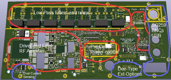
PA Board

Sections of the PA board. See also the photo below.

The PA board consists the following features:

  • 100W PA for 1.8 to 75mHz (all HF + 6mtrs and 4 mtrs. 6m & 4M might have less power)
  • Robust finals using the RD100HHF1 finals and RD16HHF1 drivers, both push-pull
  • Power control down to zero watts
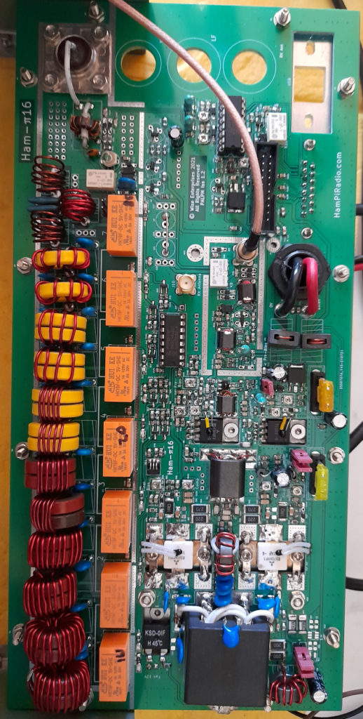
  • 7 x Low Pass Filters 160m to 4m bands
  • Each LPF has an LED to identify which LPF is selected (useful when testing…)
  • LPF bypass link for testing the PA.
  • Full break-in RX-TX-RX switching so that the receiver is on in-between CW keying
  • Metering detection, Forward power, Reverse power
  • Heat-sink temperature and Supply voltage detection. All for display on the front panel display.
  • Temperature compensation on the last 3 PA stages
  • A 15 pin Dee type connector to the rear to provide for external control of a Linear Amplifier, and other accessories
  • Temperature switch and fan control
  • This PCB is designed to fit on the rear 3mm Aluminium panel which forms the heat sink (See photos)

This internal PA works for all HF bands 1.8 to 74MHZ. For LF bands, and 2M VHF bands, an external (To be developed) module/s are needed. The current provision is made in the HamPi for this in the BPF and VFO.

Construction

If you have any design suggestions or improvements to better these construction notes and project, please do feed them to me and they will be considered and included in any further releases, and on the HamPi website.

The PA has been converted to SMD parts where possible and economical. It is quite a time consuming part of the HamPi project, so don’t rush but enjoy the process. There are still a number of parts that need to be hand mounted and as with inductors and transformers need to be would and hand mounted. Coil winding can actually become an enjoyable and therapeutic exercise if you allow it to be. Taking your time and care will reduce the risk of having any issues when testing later on.

For construction there is a BOM (HTMLBOM Bill of Materials) file that works on an internet browser making things really easy. This file will be available in the future on this web page.

Mechanical

The PA PCB is mounted on a 3mm panel which also forms the back plate of the main chassis.

Transformers and Inductors

IDCore TypePrimary TurnsSecondary TurnsNotes
T1BN-43-24028 / 0.25mm2 / 0.25mm
T2BN-43-24022 / 0.25mm8 / 0.25mm
T3BN-43-24024 / 0.3mm2 CT / 0.3mm
T4BN43-2022 CT / 0.8mm1 Coax outer (RG111 etc)See notes for building
T5T50-4310 / 1mm1 (PTFE) / 1mmSee notes for building
T6BN-61-0021 CT (Coax Outer)4 / (1mm PTFE)See notes for building
L7BN 37-4310t / 0.5mm1See notes for building
L24T50-4310 / 1mmno secondary

Final RF Transformer (BN61-002) T6 Construction:

  1. There is a huge gain to be had in not using copper or brass tubes for the construction of a final transformer. By using coax outer that is stretched so that increases the proximity of the primary to secondary turn and increases the efficiency of the transformer, meaning more power transfer, and a lot less current (which would otherwise become heat). For this reason the Binocular Core BN61-002 is used.
  2. To set up the capacitors to match this transformer on the primary a VNA is recommended recommended. While this is not essential, and the capacitor values recommended should work, if there is any variation in the capacitor or ferrite or lead lengths the result will be a poor return loss across some or all of the frequencies in use. This will result in lower output power on certain bands, and more current and heat generated (power lost) in this transformer.
  3. Use high quality capacitors, and 1000V working 1206 SMD parts are recommended. (The blue through hole ones from AliExpress are ok for discovering what values are needed, but in practice can and have burned up!)
  4. Primary turns. The Secondary (Output) is made of 4 complete turns of 18 or 20 gauge PTFE or Teflon type high temperature multi-strand wire. Choose wire that has a thinner insulation to minimise the gap between primary and secondary. A single turn is counted as a wire passing through a hole of the binocular core AND back through the other hole. When this secondary is wound there will therefore be 3 turns in-between the ends of the wires and 4 turns looping back at the other end of the core.
  5. The primary turn. The primary is one complete turn using a length of quality coax outer braid. Get some coax, RG58 or similar. Not the cheap stuff that you can see through the braid, but tightly made. Remove the rest of the coax, the inner core and outer insulation so there is just the braid. Push it together so it expands somewhat and so it can be passed through one hole, and back through the other hole of the BN-61-002 ferrite core. Use tweezers, or a tooth pick or cocktail stick to open up a hole in the braid where it is turning the corner of the return bend. Now carefully pass the 18 gauge primary wire through from one turn end and through the opened up hole. Next pass it back through the same hole in the braid but through the empty ferrite coax hole. Now continue in the same way passing the 18 gauge wire until 4 complete turns are made. This can be very tricky and a fun challenge! So have patience and enjoy doing this, and congratulate yourself when a nice tidy job is done. See pictures, they speak better than the above description…
  6. Close up the hole in the braid carefully, so as not to break the braids, completely covering the inner wire.
  7. Pull the two ends of the braid on the ends of the single turn. This tightens up the braid over the primary.
  8. Use another offcuts of braid and solder a neat tab to the centre tap of the braid on the bend (at the half-way point). This is the centre tap, and where the DC voltage is introduced to the transformer. Face the braid down as so and ‘L’ shaped tab is made and cut off so it can be soldered later on to the PCB.
  9. Flatten out the two braid on the other end and point down, (Gove them another tug to tighten it again) and tin them by filling them with solder, and cut them off, again in ‘L’ shaped tabs so they can be soldered to the PCB later on.
  10. Cut off the ends of the Secondary wire, twist and tin. Cut to the right length to solder them to the outer earth and output pads on the PCB.

Final RF Transformer T6 Matching with a VNA:

  1. This procedure may not be needed and depends on the quality of the T5 build. If a constructor wants to experiment / check the design then this is the procedure:
  2. Fit the transformer to the PCB, leaving the output (secondary) wire disconnected on the non earth end that would normally go the r Low Pass Filters. Fit an SMD SMA Coax socket temporarily to this secondary output and to ground on the PCB.
  3. Get two 1.5R resistors and two 160pF capacitors. Temporarily solder one of each R and C on the output pads (Drain) of the final RD100HHF1 / RD70HVF1 MOSFETs to one of the ground pads. This is to create a termination match ‘as if’ the finals were fitted, so that matching sing a VNA can be achieved.
  4. Calibrate the VNA and save the results.
  5. Put the capacitors in the correct holes in the pcb with their wires cut fairly short. ~8mm long.
  6. Solder the one capacitor to the TCW stub wires.
  7. If all the capacitors are making contact, ensure the VNA readout is similar to the photograph. Main points: At less than 30mHz the graph should be less than 16dB. At 50 and 70mHz there could be dips to 15dB (good) but dips of only 8 or 10dB might be possible.
  8. If the above looks good, solder the 1206 capacitors in place, and check again with the VNA.
  9. If the match is not good, find out why. Variations in capacitor values, quality, leakage and lead length are all factors, and can easily upset the matching. Experiment with values and locations of the capacitors until a good result is found.
  10. Do not pass these stages by, they are important. If you are not confident or cannot get it sorted fine a friend or radio club to help out…
  11. Note: Remember, 10dB return loss means 1/10th of the power is being reflected back into the transformer so 90Watts is being transmitted and 10 watts lost in current and heat. Another 3db, so 13dB return loss halves these figures, so 95W transmitted and 5W lost. Again another 3dB is 16dB is 97.5W transmitted and 2.5W lost, not bad at all. This is why something around and better than 15dB is a reasonable target.

More to follow… Under construction

Loading

Scroll to Top